Effect of Annealing Temperature on Microstructure and Mechanical Properties of Nanocrystalline Copper
In this paper, bulk nanocrystalline copper with a thickness of about 600 μm was prepared by electrodeposition, and annealed at 100-250 °C. The effect of annealing temperature on the microstructure and mechanical properties of nanocrystalline copper was studied. The results show that both unannealed and annealed nanocrystalline copper exhibit face-centered cubic structure; as the annealing temperature increases from 100°C to 250°C, the diffraction peak intensity of (200) crystal plane of nanocrystalline copper increases gradually. With the increase of annealing temperature, the tensile strength of nanocrystalline copper gradually decreases, the elongation after fracture first increases and then decreases, and the number of large and deep dimples on the surface tensile deformation band and tensile fracture increases; 200 After annealing at ℃, the tensile properties of nanocrystalline copper are better, the tensile strength is about 500MPa higher, and the elongation after fracture is nearly 30.5%.
1. Sample preparation and test method
Nanocrystalline copper with a thickness of about 600 μm was prepared on the surface of SS316 stainless steel by electrodeposition method, and then it was peeled off from the stainless steel surface to obtain bulk nanocrystalline copper. During electrodeposition, a SS316 stainless steel plate with a size of 100mm×60mm×1mm is used for the cathode, and a phosphorus-containing copper plate with a size of 20cm×10cm×3cm is used for the anode. Before electrodeposition, both the anode and cathode need to be acidified and degreased to remove surface oxides and grease, and then rinsed with deionized water. Electrodeposited at 25 ℃ and current density 1.5A·dm-2 for 33h, a bright nanocrystalline copper layer was obtained on the surface of SS316 stainless steel. The stripped nanocrystalline copper is placed in an annealing furnace and annealed under the protection of nitrogen. The annealing temperature is 100-250° C. and the holding time is 30 minutes.
The microstructure of nanocrystalline copper was observed by transmission electron microscope (TEM) and analyzed by selected area electron diffraction (SAD). The phase analysis of nanocrystalline copper annealed at different temperatures was carried out by X-ray diffractometer (XRD). Cut the nanocrystalline copper before and after annealing into a dog-bone tensile specimen with a size of 8mm×2mm×0.5mm by wire cutting method, and use a universal tensile testing machine under the condition of a strain rate of 4.17×10⁻²s-1 Tensile test at room temperature. A scanning electron microscope (SEM) was used to observe the tensile fracture morphology of the sample and the surface morphology near the fracture. The measurement software was used to carry out the dimple size distribution statistics on the fracture after stretching. For each sample, 100 dimples with clear boundaries were selected for length statistics.
2. Experimental results and discussion
2.1 Effect of annealing temperature on microstructure
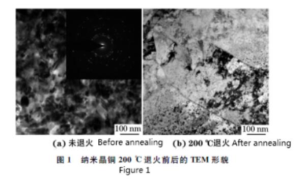
It can be seen from Figure 1(a) that the grains of nanocrystalline copper obtained by electrodeposition are equiaxed crystals, the grain boundaries are more obvious, the grain size is 20-70nm and the average grain size is about 40nm; the SAD pattern of nanocrystalline copper There is a more obvious diffraction ring, which shows that the nanocrystalline copper prepared under the condition of current density 1.5A·dm-2 has a smaller grain size and a narrower grain size distribution. It can be seen from Figure 1(b) that the nanocrystalline copper grains after annealing at 200 °C have grown significantly, which indicates that the microstructure of nanocrystalline copper has undergone significant changes after annealing.
2.2 Effect of annealing temperature on crystal structure
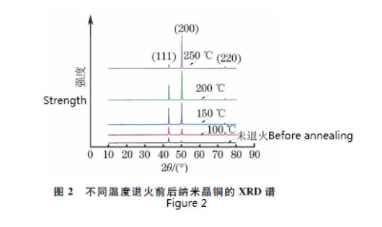
It can be seen from Figure 2 that the nanocrystalline copper without annealing and annealing at different temperatures all present a face-centered cubic structure and the diffraction peaks of copper (111), (200), and (220) crystal planes appear; the unannealed nanocrystalline The diffraction peak intensity of the copper (200) crystal plane is weak, and the diffraction peak of the (200) crystal plane becomes stronger after annealing, and as the annealing temperature increases, the diffraction peak of the copper (200) crystal plane strengthens and tends to sharpen , the half-width is reduced. It can be seen from the Scherrer formula that the grain size of the annealed sample increases.
2.3 Effect of annealing temperature on mechanical properties
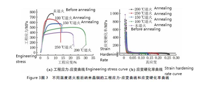
It can be seen from Figure 3(a) that the tensile strength of unannealed nanocrystalline copper is about 770 MPa, which is higher than that after annealing at different temperatures, and the elongation after fracture is about 8.6%, which is lower than that after annealing at different temperatures; As the temperature rises, the tensile strength of nanocrystalline copper decreases, and the elongation after fracture first increases and then decreases. When the annealing temperature is 200℃, the elongation after fracture is the largest. The reason why the tensile strength of nanocrystalline copper decreases with the increase of annealing temperature is that: on the one hand, driven by an external heat source, dislocations recombine through slipping and climbing, which reduces the dislocation density inside the material and weakens the ability to resist deformation. ; On the other hand, during the annealing process, grain growth leads to a reduction in the number of grain boundaries, which are an effective barrier to dislocation sliding, so the strength decreases. It can be seen from Figure 3(b) that when the true strain is about 7.3%, the strain hardening rate of unannealed nanocrystalline copper drops to 0 rapidly; when the strain hardening rate of nanocrystalline copper after annealing is 0, the corresponding true strain first increases with the increase of annealing temperature When the annealing temperature is 200°C, it decreases and reaches a maximum of about 23%, which is consistent with the change of elongation after fracture. It shows that the strain hardening ability and plasticity of nanocrystalline copper increase first and then decrease. The improvement of strain hardening ability and plasticity of nanocrystalline copper after annealing may be related to the growth of some grains during annealing: larger grains can generate more space to accommodate newly generated dislocations, thereby improving the performance of nanocrystalline copper. Plasticity; in addition, large grains can more effectively coordinate the deformation of nanocrystals, so that the internal stress concentration can be effectively released, and this coordinated deformation will also make it difficult for microvoid nucleation, thereby further improving the plasticity of nanocrystalline copper.
In summary, under the annealing condition of 200 °C, nanocrystalline copper has obtained relatively excellent tensile properties: the strain hardening ability is the largest, the tensile strength reaches 500 MPa, and the elongation after fracture is 30.5%. The annealing treatment improves the strain hardening ability of nanocrystalline copper, delays the occurrence of necking, and greatly improves the plasticity of nanocrystalline copper.
2.4 Effect of annealing temperature on microstructure
2.4.1 Effect on Surface Topography
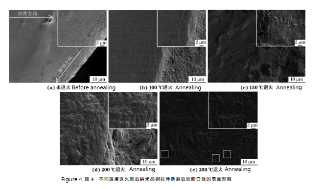
It can be seen from Figure 4 that after tensile fracture, the surface near the fracture of the unannealed nanocrystalline copper is smooth and flat. It can be seen from local enlargement that there are a small amount of furrow-like shear deformation bands parallel to the fracture direction in the area near the fracture, indicating that Unannealed nanocrystalline copper only deforms in a small area near the fracture due to insufficient dislocation mobility, and the deformation of a small area will lead to internal stress concentration of nanocrystalline copper and premature necking. After annealing, the surface near the tensile fracture of nanocrystalline copper is rougher than that without annealing, and the number of shear bands is also significantly more than that without annealing; and with the increase of annealing temperature, the deformation characteristics of the surface near the fracture become more and more convex and concave. Obviously, this shows that with the increase of annealing temperature, the nanocrystalline copper has a large non-uniform deformation in the area near the fracture, that is, the plasticity is greatly improved; but when the annealing temperature rises to 250 ° C, the nanocrystalline copper near the fracture A small amount of holes (shown in small boxes) appeared on the surface, which indicated that the nanocrystalline copper annealed at 250°C experienced stress concentration inside during stretching, which was the reason why its plasticity was lower than that after annealing at 200°C.
2.4.2 Influence on tensile fracture morphology
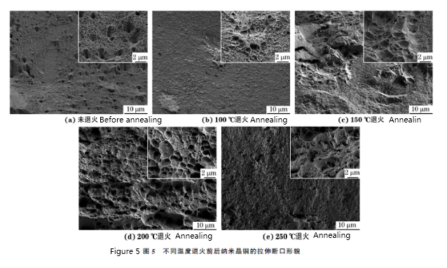
It can be seen from Figure 5(a) that the tensile fracture of unannealed nanocrystalline copper has obvious double dimple fracture characteristics, and some rod-shaped dimples with a size close to the micron scale are distributed between the small and shallow dimples. This double dimple fracture feature has been similarly reported in the literature. After annealing at 100℃, the number of small and shallow dimples on the tensile fracture of nanocrystalline copper decreases, and the number of large and deep rod-shaped dimples increases, and they are embedded in the small and shallow dimples in the form of clusters , forming a fracture morphology similar to the “core-shell” structure; as the annealing temperature continues to increase, the number of small and shallow dimples continues to decrease, and the number of large and deep dimples close to the micron level increases; in addition, at 200 After annealing at ℃, the tensile fracture morphology of nanocrystalline copper changes from the double dimple fracture characteristic of unannealed nanocrystalline copper to the fracture characteristic of uniform and alternating distribution of large and small dimples. The appearance of deep dimples means that the material needs to consume more energy to coordinate deformation dislocations during the deformation process, so that the material undergoes more uniform plastic deformation and delays the fracture of the material.
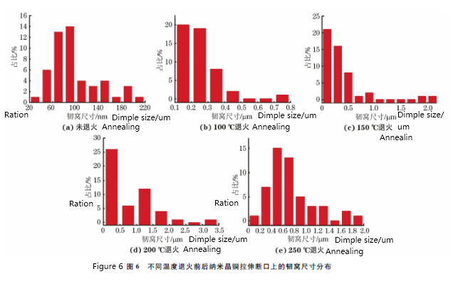
It can be seen from Figure 6 that the average size (length) of the dimples on the tensile fracture of unannealed nanocrystalline copper is 90 nm, and the average size of the dimples on the tensile fracture after annealing at 100, 150, 200, and 250 °C is 230 nm, respectively. , 360, 720, 710nm, the average size of dimples first increases and then decreases with the increase of annealing temperature; after annealing at 200℃, the size of dimples on the tensile fracture of nanocrystalline copper presents a “bimodal” structure distribution, and the size of small dimples is about The size of the large dimple is as large as 3.5 μm. This size difference makes the average size of the dimple after annealing at 200°C larger than that after annealing at 250°C; the size of the dimple on the tensile fracture of nanocrystalline copper after annealing at 250°C more evenly distributed.
3. Conclusion
(1) The nanocrystalline copper without annealing and annealing at different temperatures (100-250°C) all present a face-centered cubic structure. As the annealing temperature increases, the diffraction peak intensity of the copper (200) crystal plane gradually increases, and the half-maximum width decreases, the grain size decreases.
(2) The tensile strength of unannealed nanocrystalline copper is about 770MPa, which is higher than that after annealing, and the elongation after fracture is about 8.6%, which is lower than that after annealing; with the increase of annealing temperature, the tensile strength of nanocrystalline copper after annealing The tensile strength decreases, and the elongation after fracture first increases and then decreases. When the annealing temperature is 200°C, the elongation after fracture is the largest, which is 30.5%.
(3) After tensile fracture, the surface of the unannealed nanocrystalline copper sample is smooth and flat, and there are a few plow-shaped shear deformation bands near the fracture front, and the dimples on the fracture surface are small and shallow; with the increase of annealing temperature As the temperature rises, the number of deformation bands on the surface of nanocrystalline copper increases, the degree of deformation increases, the number of large and deep dimples on the fracture surface gradually increases, and the average length of dimples first increases and then decreases.
Equipment Composition And Details Of Large-Scale Finishing Rolling Steel Bar Heat Treatment Furnace Effect of High Energy Ball Milling and Vacuum Annealing on Microwave Properties of Nanocrystalline FeSiAl Gear Carburizing Heat Treatment Furnace Structure Composition And introduction
Contact us
Your email address will not be published. Required fields are marked *